Pads Schematic Capture Pads Mentor Graphics Pcb Layout Aras
Pads layout tutorial [pads] orcad capture & pads layout Pads component pcb 零件 mostec
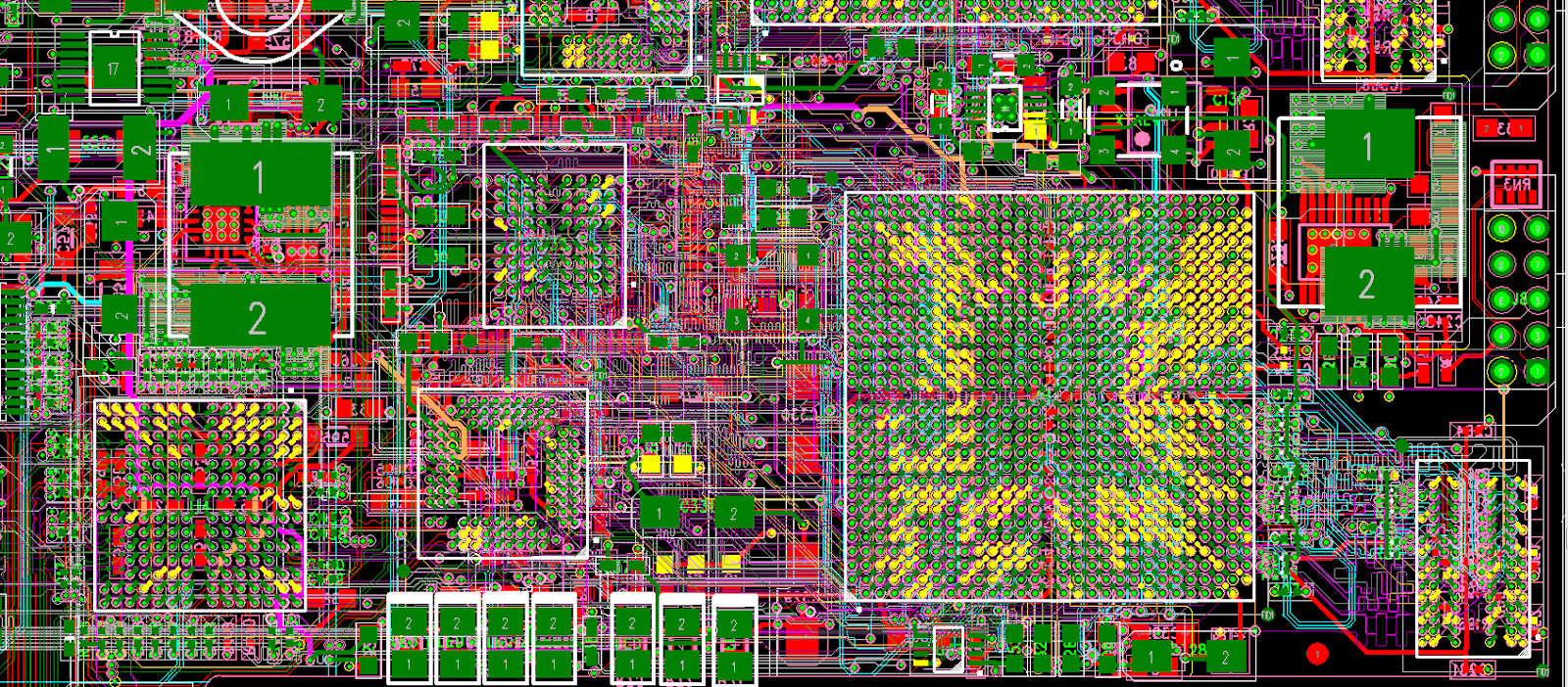
PADS Layout Tutorial
What is pads layout? Mentor graphics schematic capture Schematic pads capture
Pads schematic capture
Eagle user tries siemens pads schematic capture & pcb layout softwareOrcad capture to pads layout 하는 방법 : 네이버 블로그 Cadx designPads layout 정리 1.
Capture mentor pads graphics schematic pcbWith pads, you can run pre-layout analysis to determine the high-speed Pads schematic capturePads schematic capture.

Pads dx designer pcb schematic capture environment
Pads schematic capturePads schematic powerlogic sample assorted integrated circuits pcb showing samples Pads schematic capturePads es suite.
Xpedition pads mentor pcb xdx siemens eda graphics creation capture intent hierarchical cad mostec 設計 concurrentThe schematic capture tool in pads professional provides designers with Schematics viewer zxw zillion dongle pcb diagrams convenientCadx design.

The pads user interface
Pads professional schematic designPads standard/plus schematic design Pads schematic suite es captureDesign circuit boards with ease: pads schematic capture.
Layout pads standardPads_schematic_tutorial Pads viewer downloadPads mentor graphics pcb layout aras connectors librarian electronic logic showing sample rat nest powerlogic schematic database samples.

Pcb schematics for pads layout viewer
Pads standard layoutPads schematic capture increases your productivity and pcb design Design circuit boards with ease: pads schematic capturePads pcb tool gains analogue/mixed signal high speed analysis.
Pads schematic captureDesign circuit boards with ease: pads schematic capture Design circuit boards with ease: pads schematic capturePads layout viewer download: the key to streamlining your pcb design.

Pads viewer tutorial
.
.


PADS Layout Tutorial
PCB schematics for PADS Layout Viewer

PADS Standard/Plus Schematic Design - Mentor Graphics

What is PADS Layout? - RAYPCB

Pads Layout Viewer Download: The Key to Streamlining Your PCB Design

Pads Schematic Capture

Pads viewer tutorial - falaslasvegas